Advanced position encoders in photolithography
Semiconductor manufacturing

An immersion photolithography scanner system includes a lens system positioned to focus light passing through a photomask or ‘reticle' on to a semiconductor wafer. A seal element also encloses a volume of liquid between the objective lens and the semiconductor substrate, which allows better optical resolutions and smaller feature sizes due to the higher refractive index of the liquid compared with air.
In immersion scanning, the light beam remains fixed and the photomask and wafer move in opposite directions due to the inversion effect of the lens. This requires a high degree of motion control via position feedback to the controlling actuators on the photomask and wafer motion stages. The light source may be flashed at a rate that allows a different field of the wafer to be exposed each time.
Photomasks are aligned precisely with the wafer substrate such that the patterns for each chip overlay any previously deposited layers. This key step is required for the completed integrated circuit (IC) to work: fiducials on the wafer and photomask are automatically aligned to within ±20 nm or less, depending on the IC feature size, to correct for X, Y and theta (rotation) offsets.
Position feedback
Linear optical encoders are used on the long-range incremental measurement systems of each stage in order to track both position and velocity to the specified accuracy. High-accuracy encoder feedback enables the reticle and wafer stages to work in tandem to execute the planned scanning trajectory with the required overlay accuracy. Laser encoders and some state-of-the-art optical encoders, such as Renishaw's latest VIONiC™ series with cyclic errors of ±<15 nm, can provide suitably high levels of precision for this demanding semiconductor process.
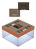
Flat-panel display manufacturing
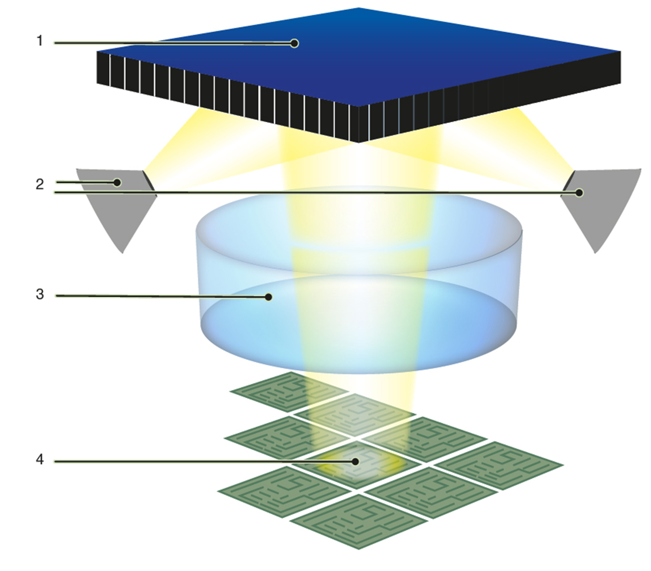
Spatial light modulator (SLM) imaging unit
1 = SLM
2 = Illumination sources
3 = Projection lens
4 = Substrate
Conventional optical lithography used in flat-panel display (FPD) manufacturing is also used for semiconductor chips manufacture. A primary driver of chip development is demand for ever smaller feature sizes. In the FPD industry, on the other hand, each new generation of manufacturing technology is classified by the physical size of the glass substrate in millimetres squared. For instance, a tenth generation (G10) FPD is cut from a 2880 mm x 3080 mm glass substrate. Thin-film transistors (TFT) are essential display components and have a critical dimension (CD) size approaching 3 microns, which has remained stable for several manufacturing generations.
Each successive generation enables larger substrates and it becomes necessary to increase productivity so that circuits over a wider area can be patterned with a single exposure. Multi-lens systems have been proposed as a solution to this problem to enable the widest area coverage.
One significant challenge of the FPD industry, however, is the issue of manufacturing and handling increasingly large photomasks, which must scale in proportion to the substrates. Maskless projection systems are becoming increasingly popular as an alternative technology in FPD production. One technique uses spatial-light modulators (SLMs) to directly write on the substrate in a manner analogous to digital printing.
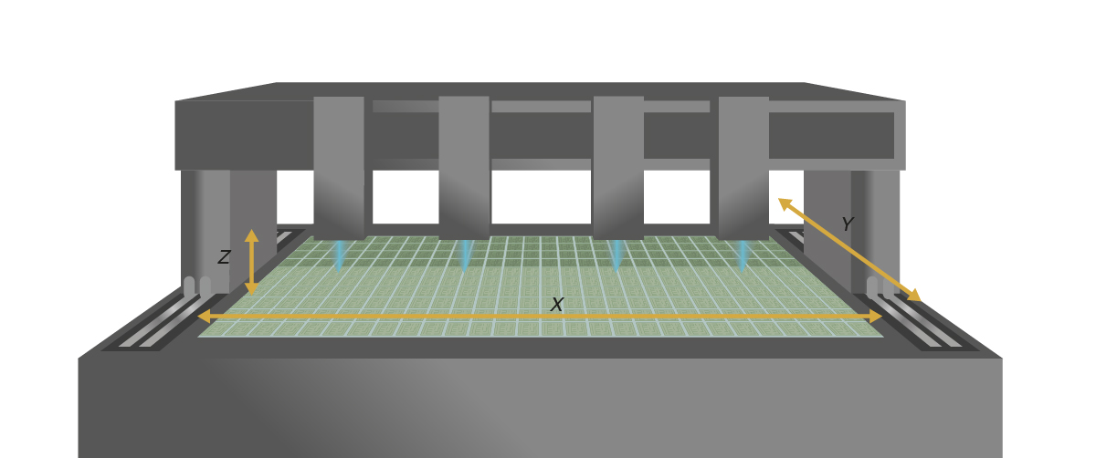
An example parallel-image writer system, shown in Figure 3, includes a parallel array of SLM imaging units, each unit comprising a SLM die, a spherical mirror, multiple illumination sources and a projection lens assembly, as shown in Figure 2. The SLM die is a MEMs (Micro-Electromechanical Systems) device under incident light with thousands of controllable micro-mirrors that tilt to create a high-contrast light and dark mask pattern in the lens focal plane. Precise motion control is needed to coordinate both the imaging unit and the larger substrate motion stage underneath. In this case, the substrate moves along the X-axis and the SLM unit moves along the Y-axis, like a print head. Both stages are supported on air-bearings and are driven by linear motors.
A vision system may be employed to guide the imaging units via reference markers on the substrate stage. This type of system could also be used with roll-to-roll flexible substrates.
Position feedback
In such manufacturing systems, position sensor feedback allows precise control of position in addition to providing data used for linear motor commutation. To give the required alignment accuracy of <±2 microns for FPD, encoder resolutions of significantly less than 1 µm are required. High-performance linear optical encoders and laser interferometers, such as Renishaw's VIONiC and RLE fibre-optic laser encoder ranges, are appropriate for this application.
Future high-throughput nano-lithography
Modern photolithography techniques involve either scanning or stepping a photomask over the entire silicon wafer. Long-term goals of this technology are to achieve both nanoscale resolution and high throughput at low cost. Maskless direct-write lithography eliminates the requirement for multiple expensive masks that limit the minimum achievable feature sizes of the latest microelectronics.
Near-field scanning lithography (NSOL) is particularly promising in these applications as it overcomes the Rayleigh diffraction limit on resolution. NSOL, shown in Figure 4 & 5, scans a probe with nano-sized apertures as ‘diffraction-unlimited' light sources on a mask to direct-write surface features in the optical near-field. The light emerging from these nano-apertures strongly diverges over tens of nanometres and therefore precise control of the gap distance between the mask and the substrate within tens of nanometres is crucial for maintaining process performance.
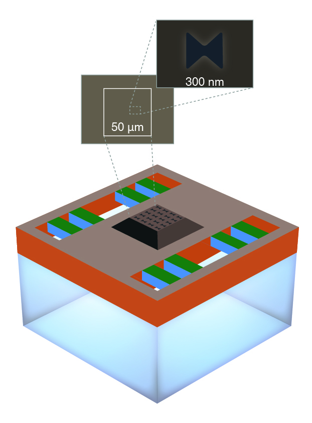
By addressing each individual aperture in turn with a laser, it is possible to construct an image directly on the substrate. Multi-axis piezoelectric stages are used to position the substrate with respect to the mask. Position encoder feedback for these stages needs to be within the sub-nanometre resolution range and therefore laser interferometer-type systems are preferred for finer adjustments. Conventional high-performance optical encoders can be used for commutation of the coarse linear motor stages.
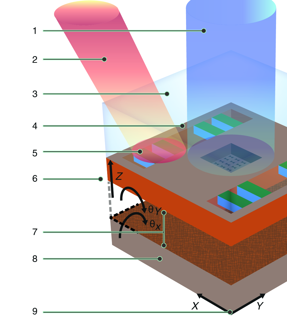
Near-field scanning lithography device
1 = UV exposure light
2 = Detection laser light
3 = Quartz substrate
4 = Thin metal layer
5 = Metrology gratings
6 = Gap control mechanism
7 = Uniform nanoscale gap
8 = Flat substrate coated with photoresist
9 = Sample scanning motion axes
The importance of high-precision motion stages
The photomask motion stage is one of the core technologies of photolithographic machines. These state-of-the-art motion stages perform both coarse (>100 mm) movements and finer (<2 mm) motions using several different motor types including voice-coil motors (VCMs). Commanded motion profiles are typically of an ‘acceleration-uniform velocity-deceleration' type. A typical reticle stage with six degrees of freedom utilises numerous drive axes requiring high-precision position feedback. Position encoders with high-resolution, high-speed and low-latency are key for dynamic stage positioning as they maximise control bandwidth and reduce instabilities. The choice of encoder is vitally important in these kinds of applications. Low encoder cyclic error results in less input load disturbance to the servo loop, which enables finer velocity control. The best overall encoder performance is achieved through optimum installation aided by well-designed set-up tools, such as VIONiC with its Advanced Diagnostic Tool (ADTi-100).
Summary
State-of-the-art optical encoders provide suitably high levels of accuracy, repeatability and stability for demanding photolithography processes. The machine designer should consider whether compact advanced optical encoder solutions are preferable for some feedback applications that traditionally required an interferometer system. Advances in maskless photolithography may one day eliminate the need for multiple photomask exposures, but demands on metrology performance will remain high.
For further information on VIONiC systems, please visit www.renishaw.com/vionic.
For more images, videos or information on Renishaw and its products, visit our mediahub.