The Casiraghi Group use Raman in the study of graphene
6th March 2015
The Casiraghi Group, located at the University of Manchester's NanoScience and Spectroscopy Laboratory, use Raman in the study of graphene.
Dr Cinzia Casiraghi is a Reader in Graphene and Carbon Nanostructures, in the School of Chemistry, at the University of Manchester, UK. She runs a research group, the Casiraghi Group, which uses Raman spectroscopy to derive quantitative information on the properties and structure of carbon nanostructures. Examples include measuring the diameter of carbon nanotubes, the width of graphene nanoribbons and the amount, and type, of defects in graphene. The Group also studies the fundamentals involved in the Raman scattering process of carbon nanomaterials. Although the Raman spectrum of graphite has been known since the 1970s, the Raman scattering process in sp2-bonded carbon nanostructures is still not completely understood. The group is engaged in activities which range from the production of graphene (and other 2D materials) to the fabrication of flexible devices made of graphene inks. Here, Raman is used as an important tool to characterise the material and possible changes introduced during the fabrication of devices. Her group works closely with the National Graphene Institute (NGI), a new £61M facility at the University of Manchester.

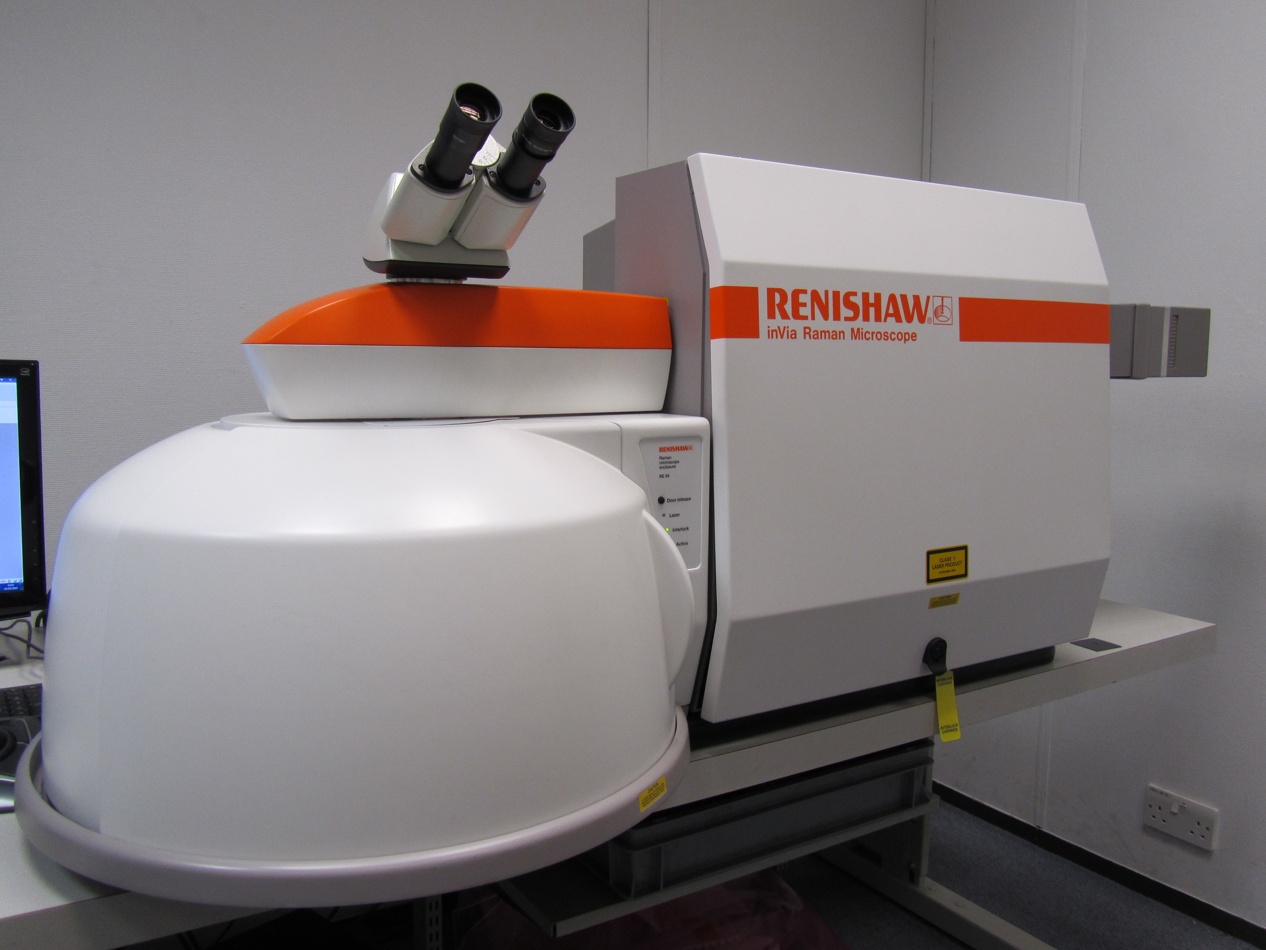
Commenting on her use of a Renishaw inVia confocal Raman microscope system, Dr Casiraghi says, “inVia is a user-friendly and sensitive Raman spectrometer which can be equipped with both mapping and multi-wavelength capabilities. Both are very useful in the study of graphene and other carbon nanostructures. Mapping allows us to collect the Raman signal from a particular area of the sample, while multi-wavelength Raman spectroscopy enables us to study if, and how, the Raman spectrum changes when the material is excited at different energies. This is very important for graphene and sp2-bonded carbon nanostructures because there are certain peaks that change in position when the excitation energy is changed. This behaviour is correlated to the properties of the material. We recently purchased a Renishaw inVia system for the new National Graphene Institute (NGI). The instrument is equipped with several laser lines, ranging from visible to near-UV (325 nm), and has a Raman mapping capability. It is very easy to change the wavelength. The UV capability is also very attractive, as the 325 nm line can be easily added to the visible lines, so it does not require buying two separate instruments. The instrument will be used for metrology studies and to set standards for graphene, in collaboration with the National Physical Laboratory (NPL).”
Continuing to describe her work, Dr Casiraghi said that the Casiraghi Group recently used the new Renishaw inVia to demonstrate the use of Raman spectroscopy as a non-destructive and rapid technique for probing the van der Waals forces between two atomically thin crystals (K-G Zhou et al, ACS Nano, 2014, 8 (10), pp 9914–9924). By performing Raman mapping on several types of heterostructures, they showed that information on the quality of the interface can be derived by looking at the changes in positions of the Raman peaks of the transition metal dichalcogenide crystal.
For further details of Renishaw's inVia confocal Raman microscope and other spectroscopy solutions, visit www.renishaw.com/raman
Image: The inVia Confocal Raman microscope