半導体
現代の電子機器には、さまざまな半導体材料が使用されています。トランジスタ、太陽電池、発光ダイオードなどの最先端デバイスは、材料特性を極限まで追及されており、きわめて均質な素材が必要とされています。ラマン分光は、半導体の研究に最適なツールです。
半導体の特徴の把握
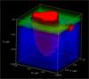
ラマンを使用すると、あらゆる半導体 (Si、カーボンベース、III-V 族、ポリマーなど) や超伝導体の特徴把握やイメージ生成が可能です。下記に挙げるような、広範な情報を解明できます。
- 化学的組成 (化合物半導体の合金の割合率など)
- ポリタイプ (4H-SiC や 6H-SicC など)
- 歪み/応力
- ドーパント濃度
- 薄膜の膜厚
- 結晶構造のタイプと配向
- 結晶品質
- 均一性と純度
- デバイス温度

簡単な分析
ラマン分析は、サンプルの準備が不要なので非常に簡単です。また、真空技術や、電子顕微鏡に付きまとう電荷の影響に悩まされることもありません。
レニショーでは、科学研究者から技術者まで、あらゆるユーザーに合うラマンシステムを用意します。
広い領域の分析
レニショーのラマンシステムは非常に大きなサンプルでも分析可能です。例えば、ウェハ全体のイメージを生成して、異物や残留応力を確認できます。
PL の特徴を把握
レニショーのラマンシステムでは、フォトルミネセンス分光 (PL) のスペクトルの取得および分析も可能です。システム 1 台で振動情報と電子情報の両方を収集できます。
オンラインシステム
レニショーのラマンシステムを製造ラインに追加することで、品質保証のためのオンライン分析を行うことが可能です。問題を早期に診断し、無駄を低減し、歩留まりを改善します。
信頼性の高い結果
レニショーのラマンシステムからは、サンプルを正確に表現する再現性の高いデータが得られます。さらに、内蔵の自動校正とヘルスチェック機能により、いつ収集したデータでも、正確に比較できます。

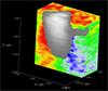
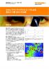
炭化ケイ素ウェハの 3D ラマンマップ
ダウンロード: 材料科学 (半導体)
-
 Application note: Photocurrent measurements on the inVia™ confocal Raman microscope [en]
When light interacts with semiconducting materials it can induce electrical currents (‘photocurrents’). These currents carry information about the electronic, optical, and charge transport properties of the material. This information is complementary to that obtainable from Raman scattering, which can identify physical changes in the material properties. This application note demonstrates the capability to simultaneously collect Raman and photocurrent data using the photocurrent mapping module concurrently with an inVia Raman microscope.
-
 アプリケーションノート: inVia ラマンマイクロスコープによる 炭化ケイ素(SiC)の分析
炭化ケイ素の特性はその結晶構造(各種のポリタイプが存在)、結晶の質、内部の欠陥の数とタイプに応じて大きく変化します。炭化ケイ素の原材料とデバイスの製造業者が歩留まりを増加するためには、これらの特性をモニターしながらコントロールする必要があります。
-
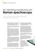
 News release: Identifying imperfections with Raman spectroscopy [en]
An article in Compound Semiconductor magazine, October 2015, describes how Raman spectroscopy allows routine mapping of SiC wafers in little more than an hour.
関連記事
inVia を使って世界のエネルギー問題解決に取り組むカリフォルニア工科大学
Caltech (カリフォルニア工科大学) は、日光、水および二酸化炭素だけを使って太陽燃料を生み出す効率的な方法の開発に取り組んでいます。この取組みは、光触媒作用と光捕獲の研究に焦点を合わせています。
2016 年度 CS 業界賞に輝いたレニショーの inVia
世界的なエンジニアリングテクノロジー企業、レニショーは、その inVia ラマンマイクロスコープで、2016 年度英国分野 CS 業界賞を受賞しました。CS 業界賞は Compound Semiconductor 誌によって企画されているもので、Web サイト (www.compoundsemiconductor.net) を通じて投票が行われます。同社は、これらを通じて化合物半導体業界に関する総合的な情報を提供しています。